Distinguished Research Chairs at the National Tsing Hua University, National Chiao Tung University, and National Taiwan University
Member, National Academy of Engineering
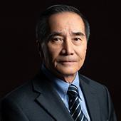
Dr. Burn J. Lin’s pioneered immersion lithography with groundbreaking innovations have revolutionized integrated circuit production to enable the continuous scaling of advanced semiconductor chips down to nano-metric feature dimensions for the most powerful computing and communication applications for the past fifteen years and foreseeable future.
Conventional “dry” lithography had been used for four decades ever since the invention of planar integrated circuits (ICs) in 1959, but encountered insurmountable barrier in late 1990s to fabricate ICs with feature sizes smaller than 65nm, owing to fundamental optical diffraction limitations. Dr. Lin foresaw an expensive dead end with the traditional projection-type lithography and proposed to use immersion (or “wet”) lithography, a novel lithographic process with enhanced optical resolution by replacing the air gap between the lens and the wafer surface with a liquid medium.
Although the concept of immersion lithography was proposed in early 80s, it was not a realizable approach. Dr. Lin created critical performance metrics and derived scaling equations for the immersion lithography systems to be fully characterized and optimized, which mapped out scaling laws for the intended super-high resolution 3D immersion optics. Additionally, he investigated and created methods to overcome obstacles relevant to micro bubble formation and the thermodynamic limit of optical diffraction via water. His inventions were proven to be feasible both scientifically and engineering-wise in applying “wet” lithography for advanced IC productions. His breakthrough inventions and enduring technical leadership convinced the entire semiconductor industry to adopt immersion lithography, continuously scaling down silicon IC tech nodes from 65nm to 7nm, delineated by using most cost-effective 193nm ArF laser source for the past 15 years. Moore’s Law has therefore been extended by 7 generations. According to IEEE’s recent statistics, at least 80% of all transistors in the world are now made with immersion lithography.
Since the invention of the integrated circuit sixty years ago, the semiconductor technology has powered the biggest industrial and social revolution in the history of mankind. As we celebrate the 60th anniversary of IC, it is appropriate and compelling to bestow the Future Science Prize in Mathematics and Computer Science to a hero of semiconductor industry, the Father of Immersion lithography, an exceptionally accomplished scientist and inventor, Dr. Burn J. Lin.